RESEARCH
The past decade has witnessed the rapid rise of quantum materials. While electrons in common solids have charge, spin and orbital degrees of freedom, and are characterized by the topological nature determined by the atomic potential on the crystal lattice, these attributes are strongly coupled in quantum materials, resulting in a high sensitivity to different forms of external stimuli, including electricity, heat, mechanical force, light, magnetic field, etc. Consequently, quantum materials show various emergent properties that are promising for the development of next-generation technologies for sensing, computing, modeling, and communication, with higher accuracy or efficiency.
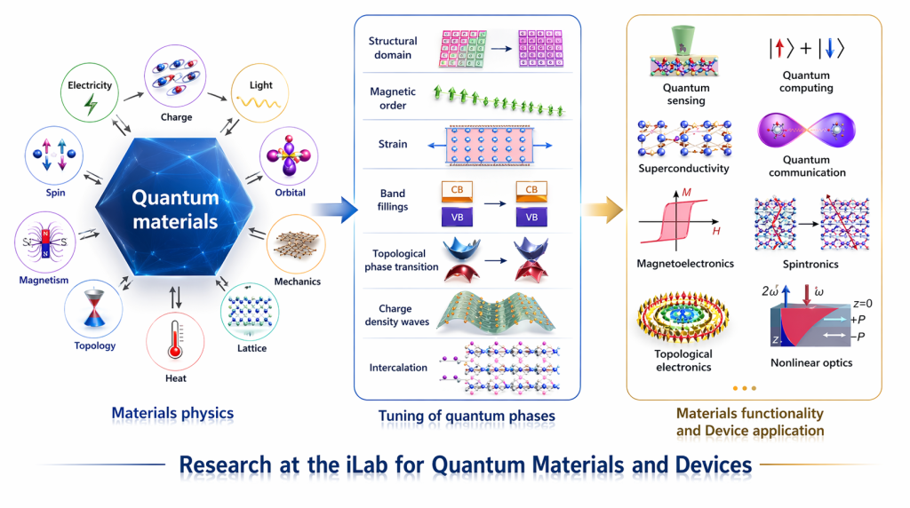
Positioned at the interface of condensed matter physics, materials science and inorganic chemistry, the Integrated Laboratory for Quantum Materials and Devices aims to address the key issues that are hindering the progress of quantum materials research towards further technological applications. Our lab combines the strength of high-quality single crystalline quantum materials growth, electrical transport characterization, and device fabrications, to promote the discovery of quantum materials with emergent properties and accelerate their transition into realistic applications in high-performance quantum devices. Our research interest and strategy can be summarized in the following figure.
The materials of focus can be categorized into the following three groups:
- Van der Waals layered crystals;
- Magnetic materials;
- Topological semimetals.
The phenomena we are interested in include, but are not limited to:
- Magnetism, including ferromagnetism, ferrimagnetism, collinear and noncollinear antiferromagnetism, skyrmion lattice;
- Charge density waves;
- Superconductivity;
- Spin-charge coupling;
- Topological phases and topological transport response;
- Strain engineering;
- Magnetoelastic coupling;
- Magnetoelectric coupling.
We employ various inorganic chemistry synthesis approaches, such as chemical vapor transport/deposition and liquid flux growth, for the development of sizable, high-quality single crystalline quantum materials. The materials characterization and device fabrication techniques that we frequently use are:
- X-ray Diffraction (XRD);
- Energy-dispersive X-ray Spectroscopy (EDX);
- Vibrating Sampling Magnetometer (VSM) or Superconducting Quantum Interference Device (SQUID);
- Atomic Force Microscope (AFM);
- Scanning Electron Microscope (SEM);
- Transmission Electron Microscope (TEM);
- Optical spectroscopy;
- Electrical transport measurements;
- Transfer Stage for 2D materials;
- Electron Beam Lithography
- Focused Ion Beam (FIB) Device Nanofabrication
- Various clean room facilities.
